Hardware Preview : Sleepy Device Development Board
Posted : 11-03-2013
How do you build reliable wireless networks when most of your devices spend most of their time in radio silence? That's what we designed our sleepy device development board to find out.
In our experience, one of the most challenging problems in designing IEEE 802.15.4 based wireless networks is dealing effectively with battery powered devices that spend most of their time 'asleep'. In order to provide a platform for testing this type of behaviour we have produced our own development boards which are optimised for battery powered operation.
The development board design shown here includes all the common functionality that will normally be required by a battery powered wireless sensor node. For reliable operation using cheap AA-type batteries, we have included a boost converter which provides a regulated 3.3V supply. This allows us to support the widest possible range of external devices during the application specific prototyping phase.
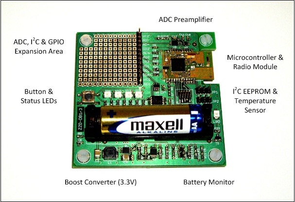
In addition to providing a regulated supply, the power management circuitry also includes battery level monitoring and under-voltage lockout. One of the problems we have observed with existing designs for battery powered devices is that they are prone to repeated spurious resets when the battery is reaching the end of its charge. The under-voltage lockout circuit addresses this by latching the microcontroller reset line when a low battery condition is detected.
Two standard I2C peripherals are also included in the design. The first of these is a temperature sensor which is used for regularly sampling the ambient temperature of the device. The second such peripheral is an external EEPROM which is used for storing firmware images during the over-the-air firmware upgrade process.
The development board is intended for prototyping a range of application specific sleepy sensor nodes. Therefore a number of GPIO lines are brought out to the board's prototyping area, together with the I2C bus. In addition, a buffered ADC input to the microcontroller is present on the prototyping header. The ADC instrumentation preamplifier provides a high impedance differential input with a sampling range of ±0.1V.
Central to the development board design is the microcontroller and radio module. This is supplied by ST Microelectronics and features their SN250 microcontroller, which is a rebranded version of the Silicon Labs EM250 device. This configuration will be used for our initial development boards, after which we plan to replace the module with our own fully integrated radio design.
The board design shown here will be included in a strictly limited release of uncertified development kits for beta test customers. We are aiming to make these kits available to interested developers later in the year, together with a number of over-the-air programmable firmware images that allow the boards to be configured for a range of different applications.